
December 2023 FAQ: Die-to-Wafer Bonding
 Take a look at some of our most frequently asked questions:
Q: Does Integra offer die-to-wafer bonding?
A: Yes we do, primarily for SiPho typically utilizing a 3-5 die onto an SOI wafer. We use atmospheric type instead of the conventional vacuum type plasma.
Q: Are there any concerns with Die-to-wafer bonding?
A:
- Surface contamination kills bond ability
- Surface smoothness - < 0.5nm
- Preplanning during fabrication is key
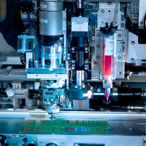
Q: What equipment does Integra use?
A: BESI 2200 Evo Plus
Q: What type of environment do you have for these processes?
A: Class 1k cleanroom / Class 100 equipment
Q: What is the throughput of the system?
A: Bonding capability up to 500 dies per hour
Q: What is the placement Accuracy?
A:
- Placement accuracy <XY>: +/- 7µm (35µm w/o pattern on die/wafer) - Placement accuracy <theta>: +/- 0.3⁰deg
- AOI prior to die placement = higher yield
- Optional Laser mark for die traceability
- FA Metrology: CSAM / Pull Test / *Surface Roughness / *SEM. (*) = Outsourced
Q: Bonding Materials:
A:
-
Material: Si / Silicon-On-Insulator (SOI)
-
Wafer size: 50~200mm
-
Thickness: 0.4~2.0mm
-
Surface roughness: Ra <0.5nm
-
Temperature: 200~1000⁰C. / Nom. 550⁰C
Q: What are the Die parameters?
A:
-
Material: InP, GaAs , BTO & TFLN (devel)
-
Die size: 0.5~50mm
-
Thickness: 0.1~7.0mm
-
Surface roughness: Ra <0.5nm (CMP req.)
-
Edge chipping: <5µm
-
Temperature: 200~1000⁰C. / Nom. 550⁰C
Have more questions? Let us know: sales_inquiry@integra-tech.com