
November 2023 FAQ: SET-NA 150 Bonding
 With flip chip pitch capabilities down to 8µm the FC150 will enhance our capabilities for Heterogeneous Integration and Chiplet Assembly.
Take a look at some of our most frequently asked questions:
Q: What are Integra's NEW bonding capabilities?
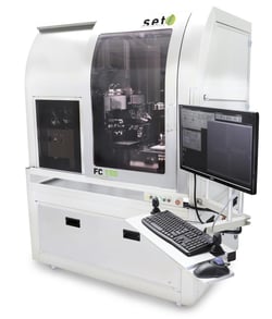
A: Integra Technologies recently added a FC150 Automated Die/Flip Chip Bonder to its line up at their Milpitas, CA location.
Q: What materials does the FC150?
A: The FC150 accommodates a wide variety of materials, including extremely fragile materials such as GaAs and HgCdTe allowing easily changed bond processes.
Q: What are some of the benefits of the FC150?
A: Some of the benefits include:
- ± 1 µm post-bond accuracy and 20 µradian leveling guarantee high yields on the most advanced products
- Semi-Open Confinement Chamber for Oxide Reduction (option)
- Air bearing construction on a granite structure ensures long-term stability and reliability
- Compression, Z-control and temperature profiling, together with process monitoring, maximize process control
- Optical automatic leveling and alignment enables hands-off operation for production applications
- Nanoimprint Lithography option with Hot Embossing or UV-NIL process without compromising the bonding capability
Q: What is the FC150 application range?
A: Chip-to-Chip, Chip-to-Substrate Bonding, Chip Stacking, 3D Interconnect, Optical Components and Photonics Device Packaging, MOEMS, MEMS, MCM, and Nanoimprint Lithography
Q: What are some of the FC150 capabilities?
A: Capabilities include:
- Bump pitch down to 8µm
- Thermo Compression bonding
- Conventional Die Attach
- Ultrasonic bonding
- Placement tolerance of 1µm
Find out more by downloading the General Guide for Assembly Services
Have more questions? Let us know: sales_inquiry@integra-tech.com