
November 2020 FAQ: Flip Chip
Take a look at some of our most frequently asked questions:
 Q: What is a Flip Chip Package?
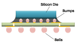
A: Essentially, the name “Flip Chip” describes the method used to connect a semiconductor die to a substrate: The dies are bumped and then “flipped” onto a substrate, hence the name “Flip Chip”.
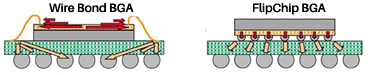
Q: What are the typical benefits of a Flip Chip device vs. a wire bonded device?
A: Flip Chip package technology offer a range of benefits including:
- High pin count
- High signal density
- Better power dissipation
- Low signal inductance, and good power/ground connectivity.
- Ideal for high speed interfaces (including RF) that wire bonds cannot support
Q: What is a Flip Chip substrate?
A: Flip Chip substrate is in essence a small Printed Circuit Board (PCB) located inside the package.
- Substrate design consists of layout of all signals from the package external balls to the bumped internal pads. It is because of a more direct path on the substrate (as illustrated below) that gives flip chip some of its advantages
- Substrates can be made by different PCB materials: laminate, build-up, ceramic, and more. Substrate layout design rules vary from different suppliers.
- Substrates can consist of many layers ranging from 2-18 layers to allow proper routing of all signals for enhanced device performance
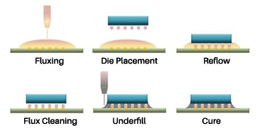
Q: What are the Assembly Steps of a Flip Chip Device?
A: In order for the chip to be connected or mounted to a substrate, the die is turned or flipped over and brought into alignment with the pads located on the substrate. There are six (6) key process steps: Fluxing, Placement, Reflow, Flux Cleaning, Capillary Underfill, and Cure.
Q: What are some of your Assembly Guidelines for Flip Chip Devices?