
CORWIL Technology successfully processes a number of materials through its wafer processing facility. While Silicon is the majority of material processed we’ve been seeing increasing trends in such materials as SiGe and GaN, as well as GaAs and InP. Each material, wafer size, and customer specification requires attention to detail and careful recipe cultivation, as well as specialized grinding and cutting tools. CORWIL’s standardization on DISCO equipment has allowed us to work closely with our vendors and be able to process multiple materials on different machines.
Backgrinding: CORWIL uses automated and semi-automated Disco equipment and grind wheels to process wafers. Speeds, grind wheel grits, and selection of appropriate WSS (wafer support system) tapes all play a role in processing exotic materials. Through repeated process verification activities, we select grind wheels and parameters that are suitable for each wafer’s specific characteristics resulting in the optimal grind conditions.
Optimal grinding conditions enable low-load grinding for both coarse and fine grinding by decelerating the feed speed of the grinding wheel spindle as the final finishing thickness is approached. Further, applications such as accelerating at the wafer vacuum table while decelerating the spindle rotation speed are effective as countermeasures to reduce edge chipping.
The following are some considerations when backgrinding some different materials:
- Grinding of GaAs (Gallium Arsenide) wafers tends to cause plucking (holes made by peeling) or scratching on the surface. In addition, depending on the difference of the wafer manufacturing process, the process ability of the GaAs wafers varies.
- SiC (Silicon Carbide) is a very hard material and extremely difficult to grind. Process time is much slower compared to Si. Using Disco’s GS08 series grind wheel, high quality SiC processing is possible for this extremely hard material. .
- InP (Indium Phosphide) Optimization of wheels and processing parameters enables high quality processing of InP used in high-speed devices. Selection of optimal processing parameters improves the condition of the processed surface compared with the traditional methods.
- Grinding of BSM (Backside Metallization) Au (gold), Ag (silver) and other exotic metals can be removed from the backside of wafers by utilizing special Disco grind wheels coupled with optimum grinding parameters and interval dressing.
The following pictures are special III-V backgrinding processes developed by CORWIL. GaAs and InP wafer diameters ranging from 3-8 inch mounted on WSS tape or sapphire carriers can be thinned to 100µ or less succesfully.
|
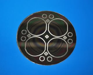
6-inch GaAs wafer mesa etched before grind, process development for ultra stable laser optics by Crystalline Mirror Solutions |
GaAs mesa singulation after grind, in this case up to ~50-mm diameter die generated via an "etch-to-core" process |
|
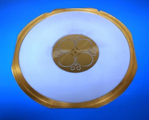
GaAs wafer portions mounted on sapphire |
GaAs wafers thinned on sapphire carriers |
|
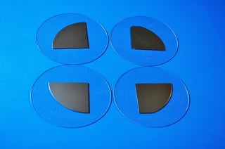
100mm GaAs wafers thinned on sapphire |
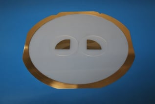
InP devices mounted and thinned on handle |
|
InP wafers mounted on WSS backgrind tape |
InP wafers “gang” mounted and thinned |
Dicing: Dicing saws use dicing blades to cut silicon, glass, and ceramic work pieces with a high degree of accuracy. Fully automatic dicing saws perform the entire process sequence: loading from the cassette, alignment, dicing, cleaning/drying, and unloading to the cassette, in a completely automated fashion. CORWIL utilizes different dicing blades and saws as well as advanced recipe development to successfully dice silicon, III-V materials and other exotic materials such as Sapphire.
Backside chipping caused during the dicing process tends to increase on exotic materials and thin wafers. Finer grit blades and the use of surfactant lubricity can reduce backside chipping. In general, a finer-grit blade imparts less of a shock to the work piece, thereby reducing backside chipping. DISCO's dicing blades are used with dicing and cutting saws to groove, cut, and dice silicon, compound semiconductors, glass, ceramics, crystals, and almost any other material. They are one key to DISCO's excellence in Kiru (dicing) processing
The following are some considerations when dicing different materials:
- Dicing SiGe: While very similar to dicing Silicon, Silicon Germanium wafers have a number of nuances that call for careful development of dicing recipes and use of alternative blades. We see increasing use of SiGe by our customers and have developed techniques to enhance edge quality of dice.
- Dicing GaAs - During dicing, breakage and cracking can easily occur in the GaAs wafer because the material is very brittle. A combination of an ultra-thin diamond blade and an aluminum hub provides enhanced operation efficiency and stable cutting results. In combination with DISCO's vast application knowledge, these blades provide excellent cutting results when dicing silicon wafers and compound semiconductor wafers such as GaAs.
- Dice before Grind – DBG: CORWIL has successfully processed a number of different materials using the DBG process including SiGe and GaAs. DBG reverses the usual process of fully dicing the wafer after grinding. In DBG, the wafer is first trenched, or partial-cut, to a depth greater than the final target thickness. The wafer is then thinned to the final target resulting in die separation. After grind, the wafer goes to the in-line DBG Mounter, which mounts the wafer and gently peels off the protective grinding tape, completing the process.
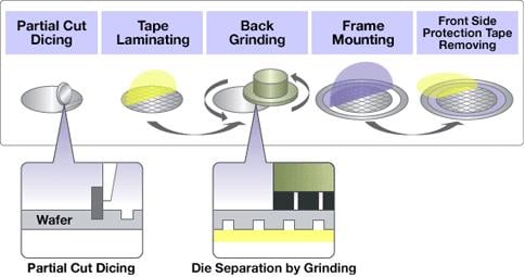
Because the die are singulated at the final target thickness, wafer-level breakage is greatly reduced. Additionally, as a result of the die separation occurring during the grinding process, the backside chipping associated with thin-wafer dicing is kept to a minimum. DBG can also provide improved die strength depending on the application. For these reasons, DBG is an excellent process for processing wafers with high-quality backside requirements.
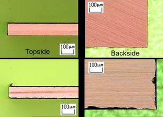
|
DGB
No DGB |
 |
Scribe and Break: CORWIL also processes die using scribe and break technology. This type of technology works well with brittle materials such as Indium Phosphide and GaAs.
The following is an overview of our guidelines for our scribe and break process:
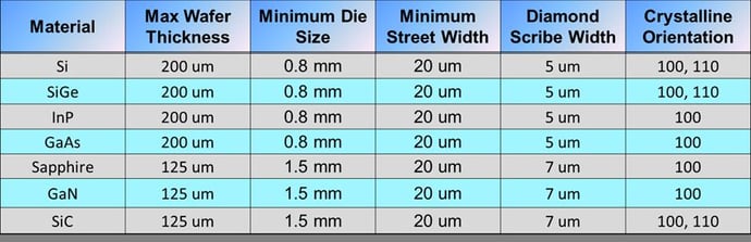
Some Caveats of our guidelines:
- Thicknesses greater than the specified optimal conditions will be evaluated by CORWIL Engineering
- Street widths narrower than specified will be evaluated by CORWIL Engineering
- Maximum wafer size is 5”
- Irregular shapes and wafer fragments and portions can be processed.
CORWIL Technology uses world class equipment and processes to process Silicon, III-V and other exotic materials. CORWIL’s work with Disco, our customers, and a long history of recipe development through Design of Experiments ensures our customers’ continued satisfaction by consistently providing high-quality results.
For more information on this or any of CORWIL's other services please give us a call at 408-618-8700 or fill out our Quote Request Form.
Click to edit your new post...