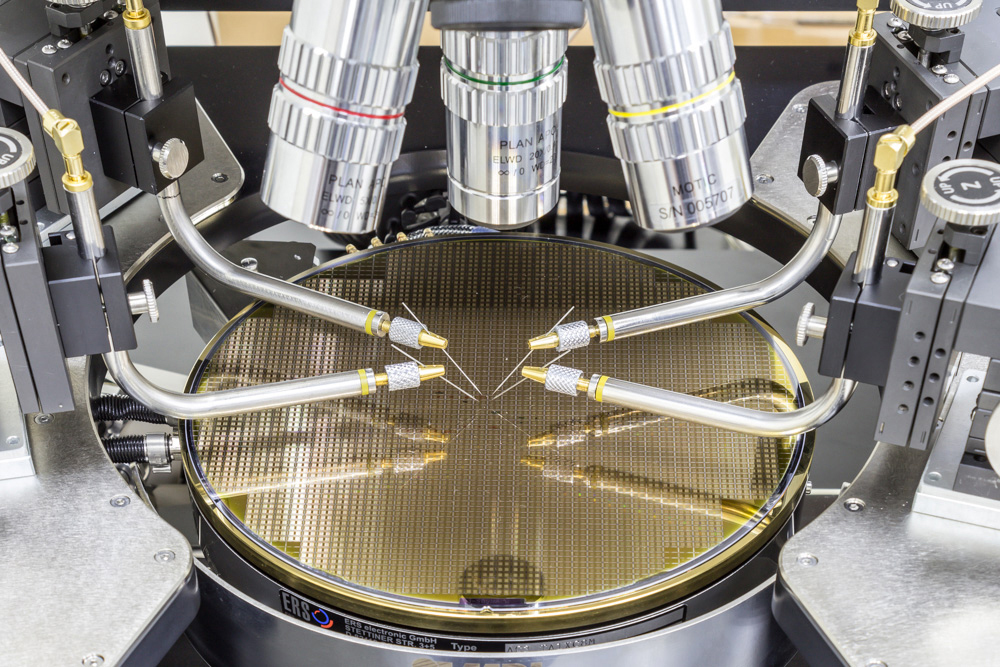
Wafer Probe
Integra Technologies has the engineering expertise, specialized equipment, and robust processes to fully support all aspects of semiconductor wafer probe services. Our comprehensive capabilities include custom test software development, probe card design and fabrication, probe station configuration and optimization, debug, and high-volume production probing.
With a team of experienced engineers and technicians, we ensure precise alignment, accurate data capture, and reliable results at every stage of wafer-level testing. Whether you're validating early designs or scaling to full production, our wafer probe solutions are built to deliver speed, accuracy, and yield optimization—all under one roof.
Experience with all probe card technologies including:
- Cantilever: 1- 16 sites up to 800 probes
- Vertical: Multi site up to 64 sites
- Membrane: Multi site
- MEMS probe cards
- RF probe to 40 GHz and higher
- Wafer probing -55°C to +125°C
- Elevated probing up to 180°C
- Singulated die probe, -55°C to +125°C, pin count to 8000+ pads
- Bumped or unbumped wafer probe
Summary of Probe Capabilities:
- Known Good Die (KGD)
- Wafer Level/Chip Scale Packaging (WLP or CSP)
- Bumped or copper pillar wafers
- Tight pitch aluminum or gold pads
- Thin wafers
- Digital, Mixed Signal and RF probe
- 2” to 12” wafer capability
- Probe card design, fab and verification
- Al, Au pads and Pb, Pb free bumps
- High Z force chuck
- High pin count, fine pitch
- Multi site
- RF probe (Membrane, Coax or custom solutions)
- N2 and vacuum wafer storage
- Data analysis capability
- High volume production probe
- 5 mil thick wafers
- 20+ years of wafer probe experience
- 100 million plus die probed
- 24x7 production capability
- 25+ test engineers
Wafer probe data analysis throughout your startup and ongoing production probe:
- Wafer Map Conversion
- Retest of defined bins without full wafer reprobe
- Custom mapping for inkless assembly
- Onsite custom format solutions for inkless assembly
- Assembly back to production map conversion
- Wafer inspection map conversion to electrical test maps
- Wafer Analysis
- Composite Mapping
- Multi site comparison
- Integration to Galaxy® software